
Electronics production
-
Individual Assignment:
- Make and test a microcontroller development board.
-
Extra credit:
- Personalize the board.
- Explore alternative fabrication processes.
-
Group Assignment:
click here
- Characterize the design rules for in-house PCB production.
- Send a PCB out to a board house.
The group assignment for this week involved characterizing the design rules for the in-house PCB production process. We aimed to mill the traces on the PCB using both the Roland Modela MDX20 and the Trotec Speedy 400 flexx Fibre Laser Engraver. Here are the results:
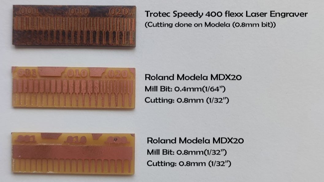
Milling machine ( Roland MDX 20 )
In the fabrication laboratories (fab labs), our standard approach for PCB production involves the utilization of the milling machining technique. This method enables individuals to create PCB prototypes akin to printing on paper with a conventional printer. To facilitate PCB milling, our fab lab is equipped with a Roland MDX 20 3-axis milling machine. This machine serves as a versatile milling apparatus suitable for crafting PCBs alongside other milling applications.

Quentorres board
The perfect combination of a versatile programmer and a beginner-friendly hello board, Quentorres, originated from the innovative mind of Quentin Bolsée and redesigned by Adrián Torres. Its inception occurred during the 2024 Instructors Bootcamp held in León.
Quentorres is equipped to program the latest AVR Series 1 and 2 devices, such as Adrianino, as well as ARMs like SAMDino. Featuring a button and an LED, it serves as an excellent tool for learning programming languages such as C, Rust, Go, Micropython, and more. Additionally, it offers breakout pins for seamless connectivity with external components.
For this week's assignment, the provided file was designated for milling purposes. To personalize my identity within that PCB, I simply appended "MJ" to it using the GIMP software.
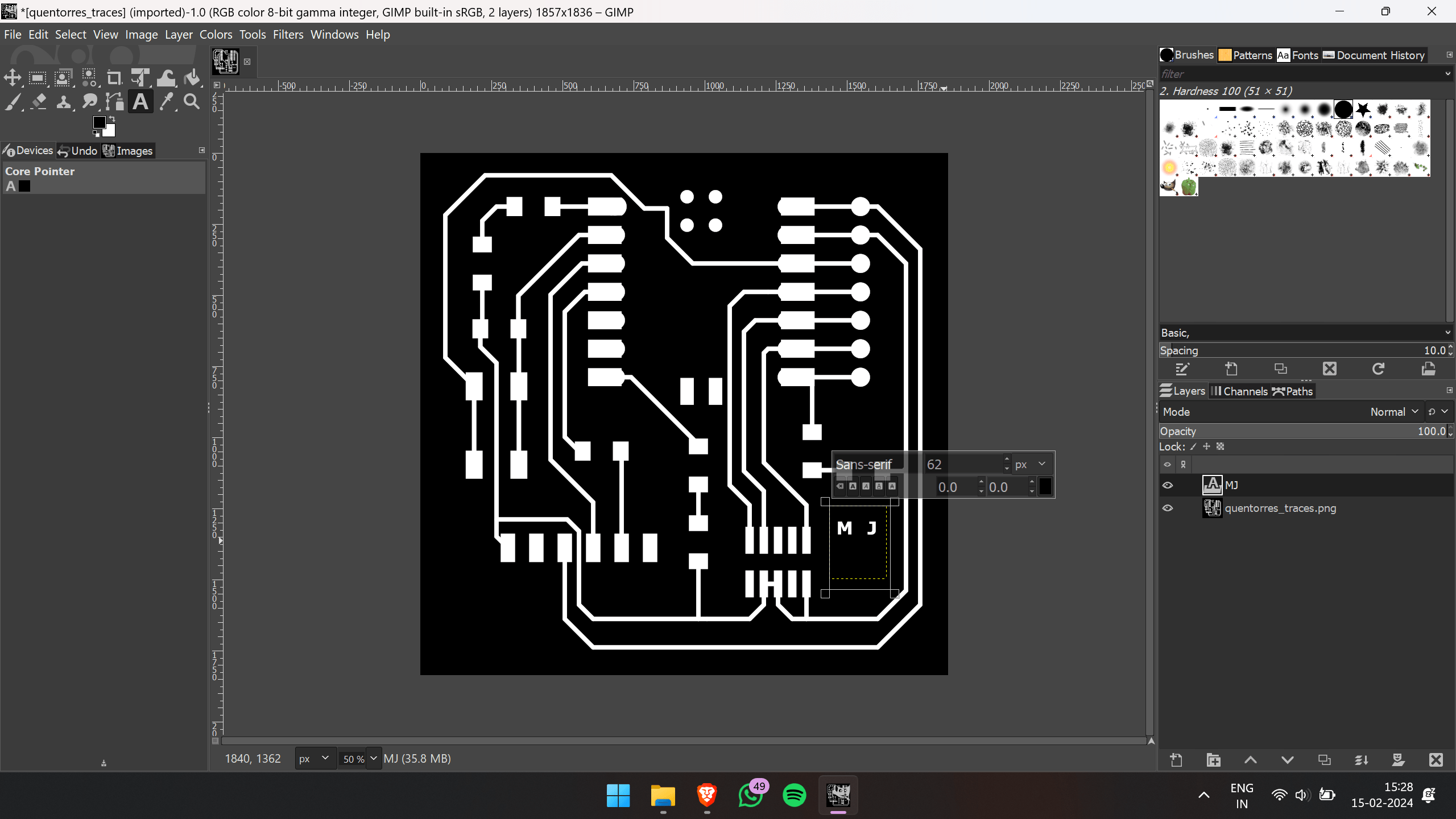
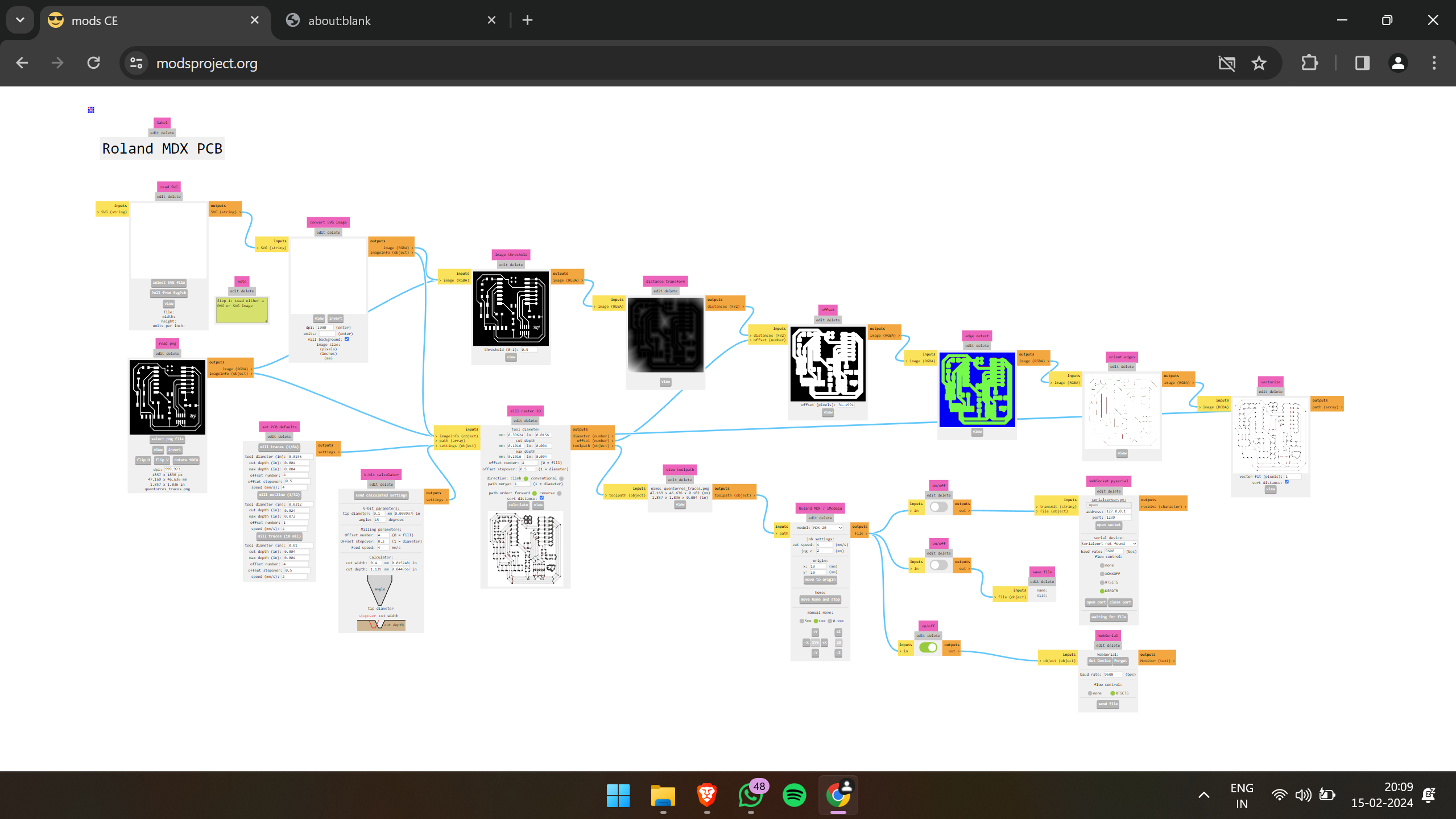
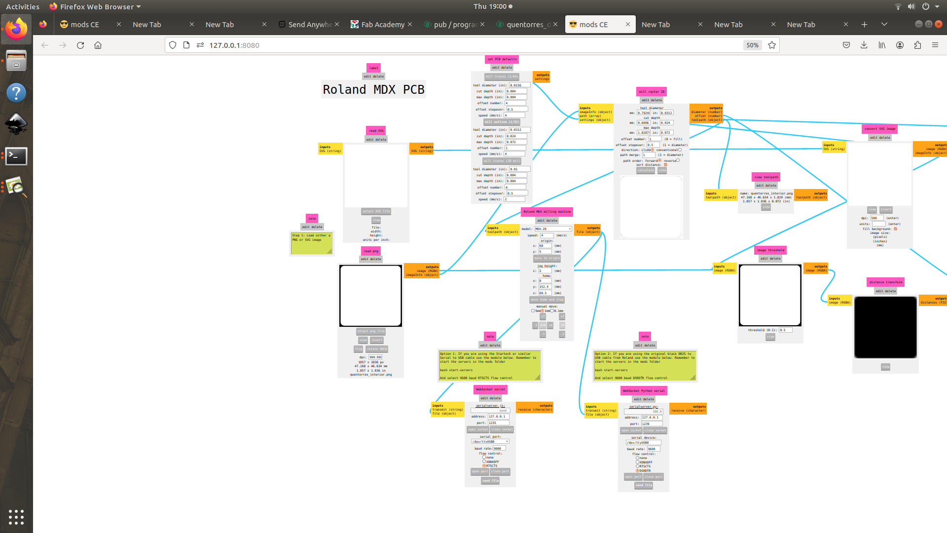
For milling the PCB, only the PNG image is necessary. Thus, I exported the design as a PNG file directly. Subsequently, I utilized the Fabmods platform to upload the PNG file for milling. Following the milling process, I proceeded to upload the drilling file, and once completed, I uploaded the cutting file for execution
For tracing the traces, start by adding the mill PNG file to the modes. Then, set the DPI to 1000 and establish the appropriate origin. Afterward, select the bit you intend to use; for this task, I used a 1/64 bit. Once selected, click on "calculate" and send the file to the machine.
For drilling the holes, swap the bit PNG file with the drill file. Change the bit to 1/32 and then send the file.
For cutting the PCB, I utilized the same 1/32 bit and swapped the PNG file for cutting the PCB.
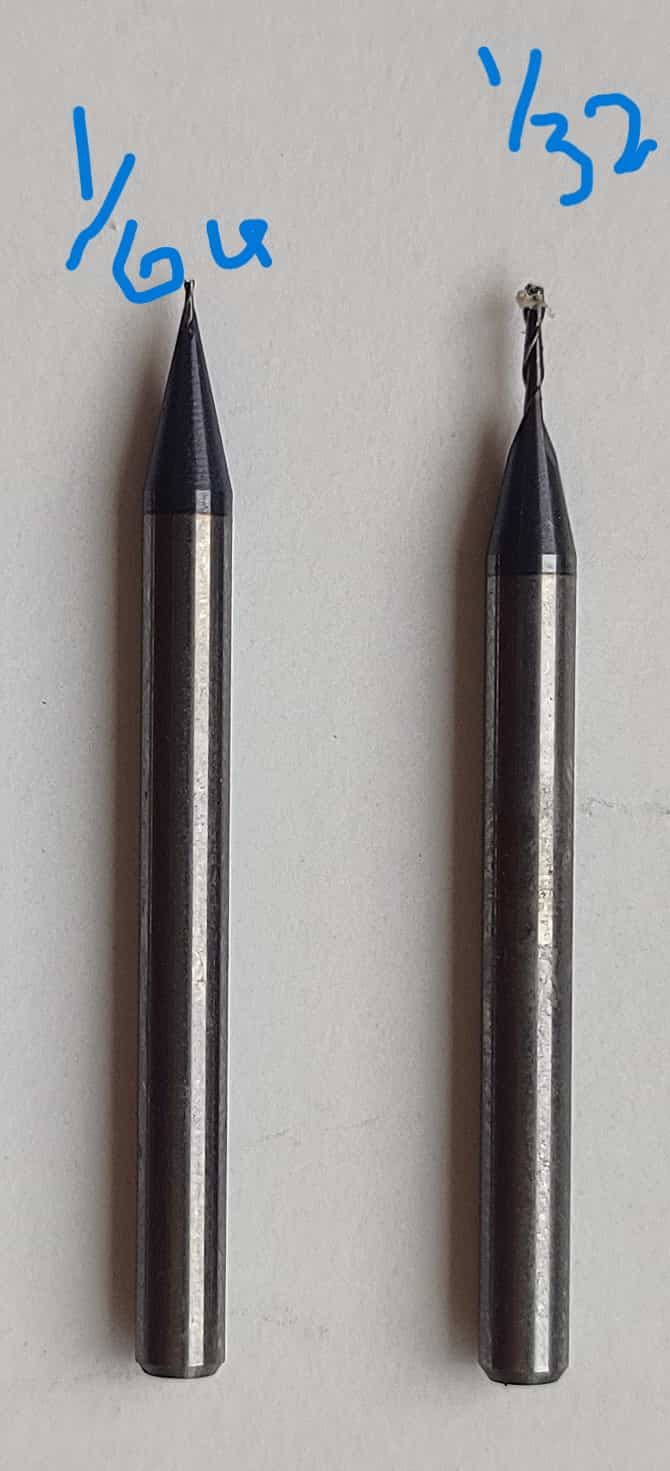
For milling purposes, we employ a 1/64 bit, whereas for cutting and drilling, a 1/32 bit is utilized. It's crucial to handle these bits with utmost care, as they are delicate and prone to damage. Here are the bits
Here's a brief clip showcasing the milling process
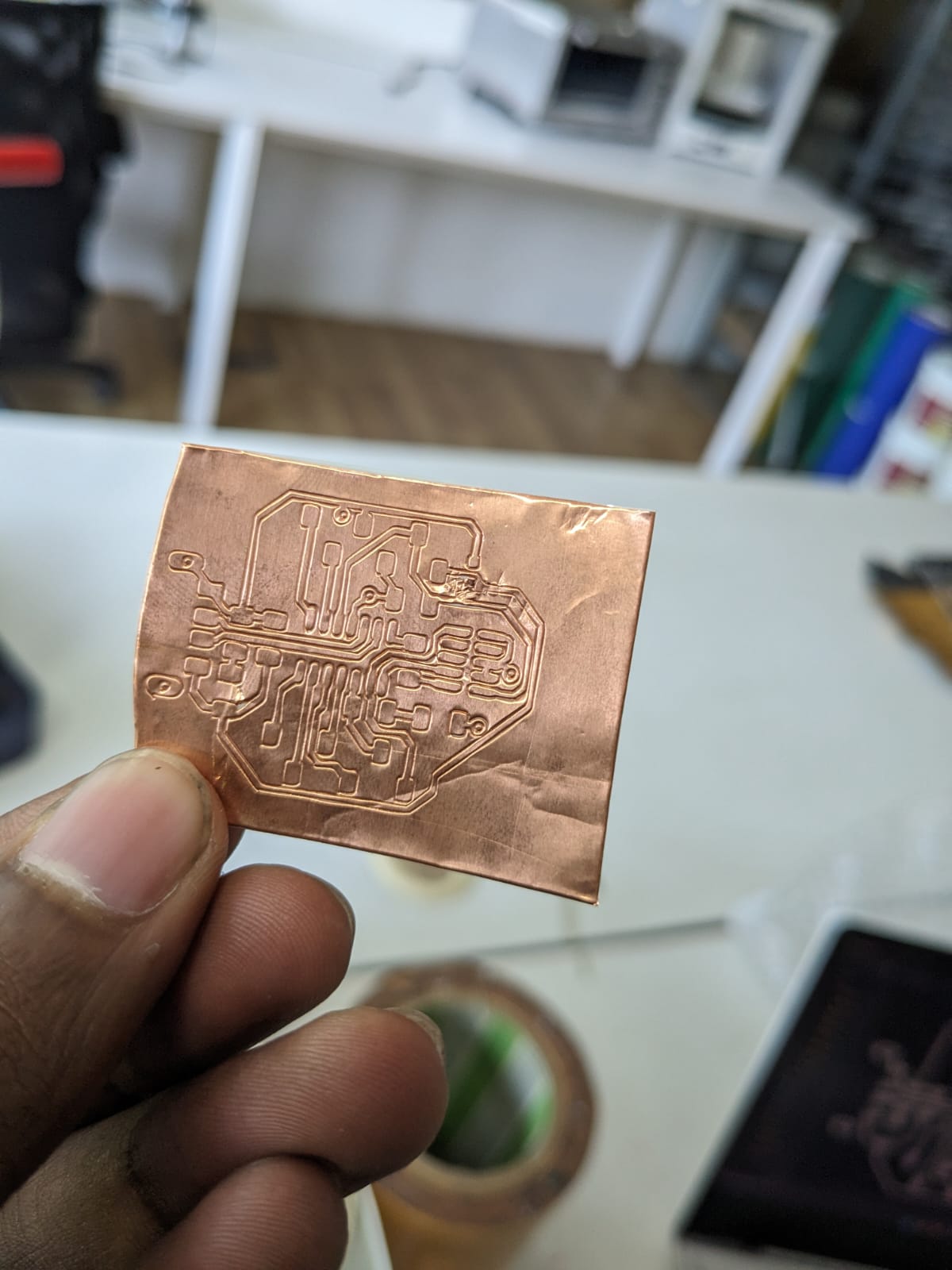
During the milling process, an oversight on my part led to the bit not being securely tightened, resulting in slight damage to the PCB tracing. Fortunately, I promptly noticed the issue and paused the machine to tighten the bit adequately. Despite this action, a portion of the PCB did sustain some damage.
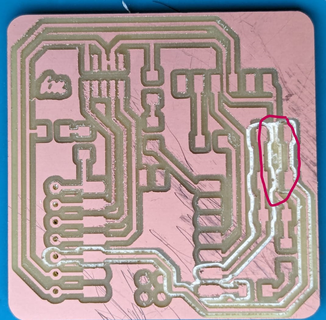
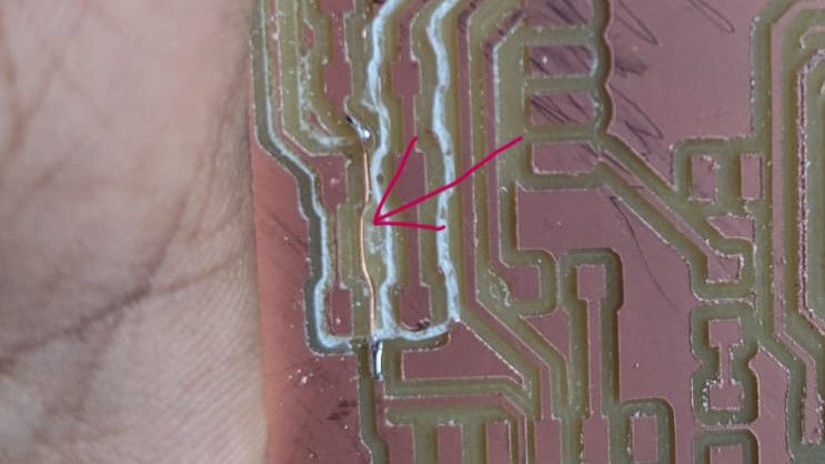
Instead of remilling the PCB, I opted to salvage it by adding a jumper wire across the breakage in the connection. This approach aimed to maintain the PCB board's sustainability as an engineer.
Here's the successful outcome after implementing the jumper wire to bridge the connection breakage
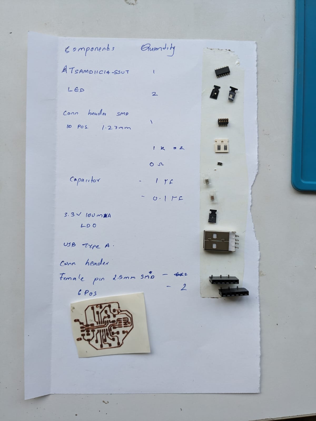
Following the successful repair of the PCB, I proceeded to gather the required components from our inventory.

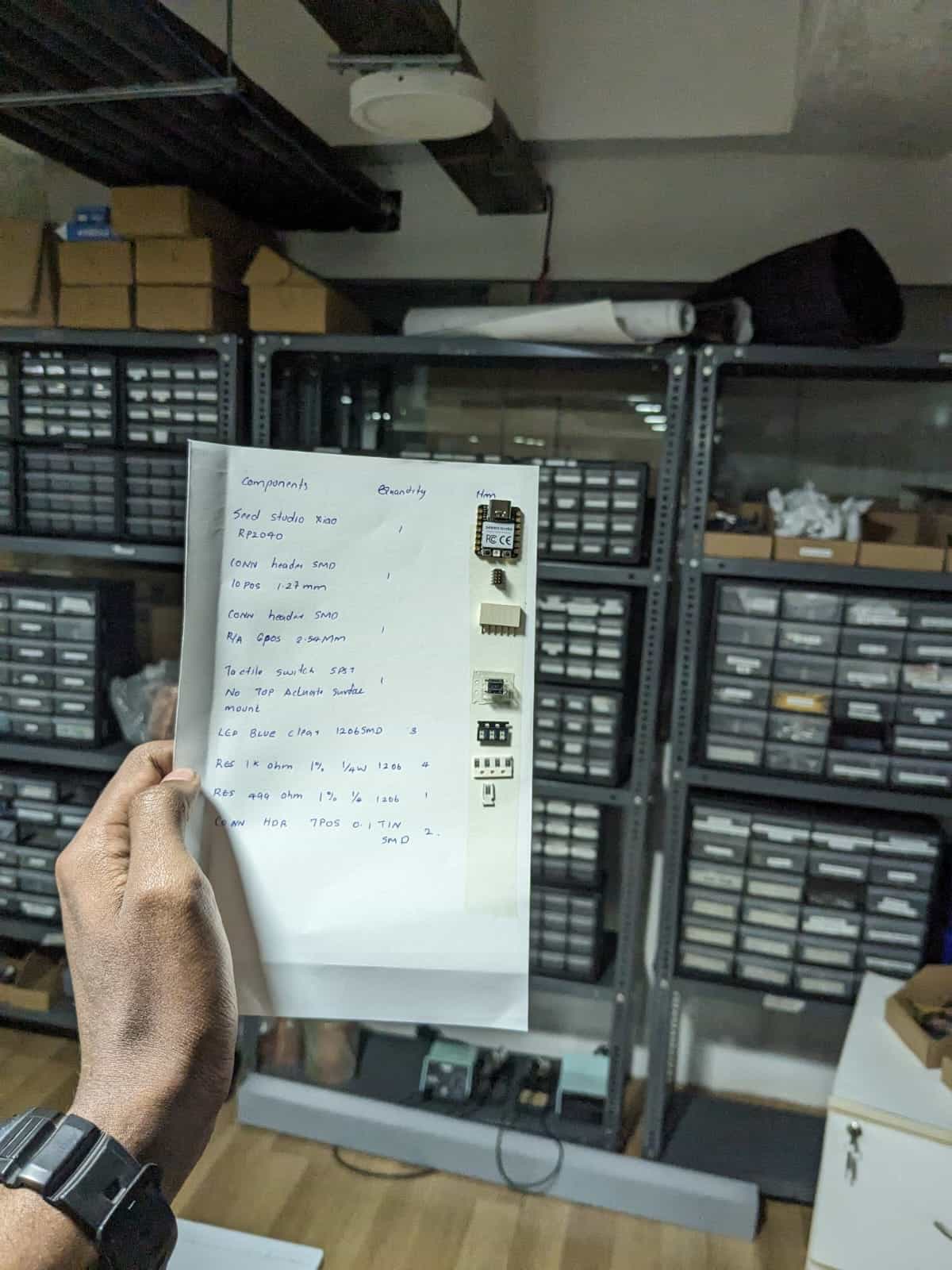
After successfully gathering the necessary components, I transitioned to the electronics workbench and commenced soldering the components using the soldering station. Drawing from my previous experience in soldering, the process was not as challenging as it might be for others.
Safety Measures for Soldering:
- Ensure adequate ventilation in the soldering area to prevent inhalation of fumes from the solder and flux, which can be harmful. Consider using fume extractors (fans) or working near an open window to improve air circulation.
- If you are working in a poorly ventilated space, wear a mask to protect yourself from inhaling harmful fumes.
- Utilize tools like tweezers or clamps to securely hold components in place, keeping your fingers away from the heat of the soldering iron.
- Always return the soldering iron to its stand when not in use; never leave it unattended while it's hot to avoid accidents or injuries.
- After soldering, remember to wash your hands thoroughly to remove any residues and prevent ingestion of harmful substances
These are the tools I used for soldering
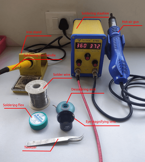
Image courtesy: Saheen Palayi
From there, I began the soldering process

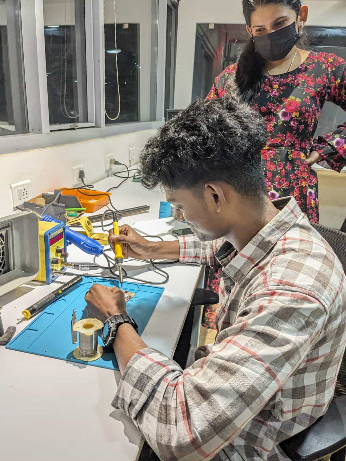
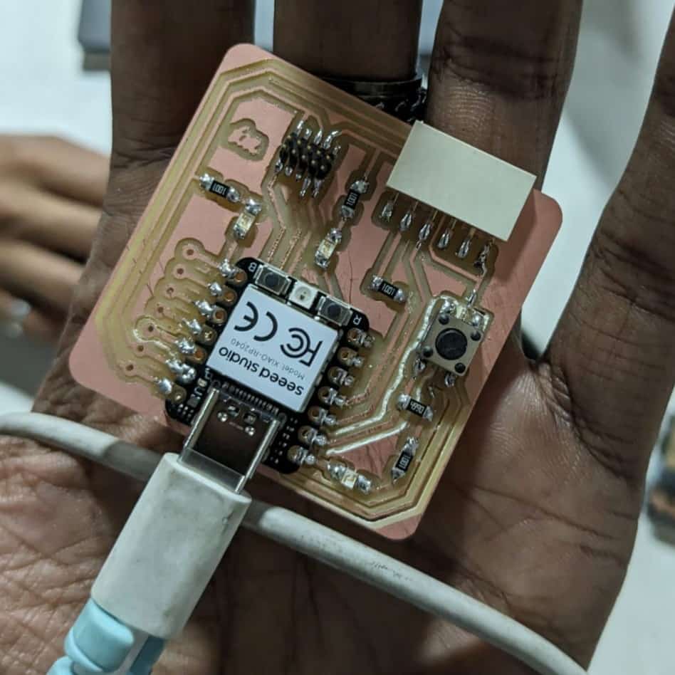
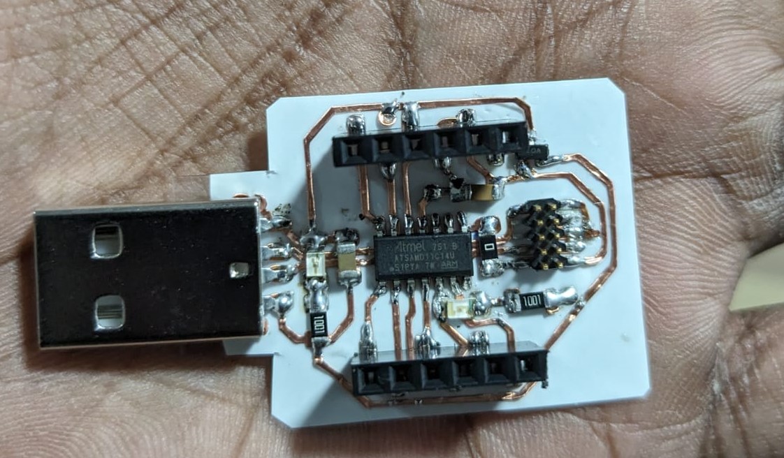
Here's the result after successfully soldering the components into place.
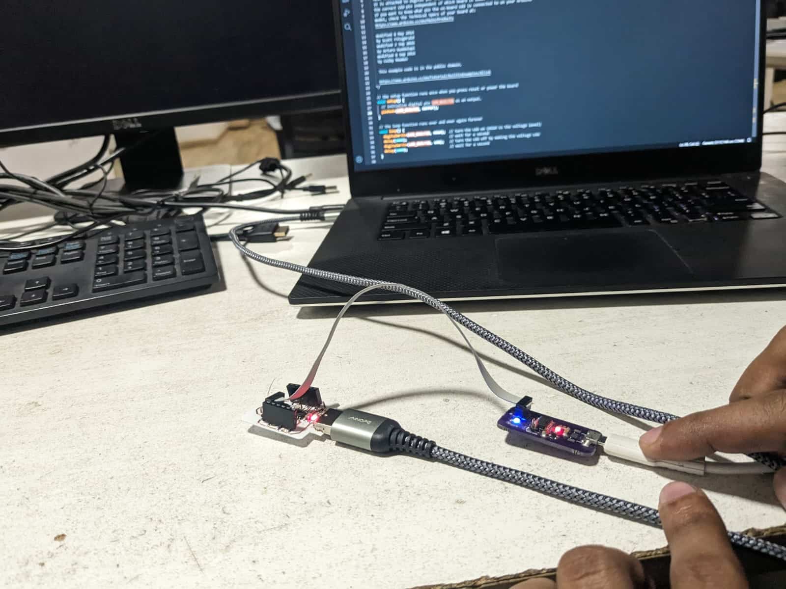
Before proceeding with the code entry, I needed to configure the Arduino IDE platform to accommodate the specific requirements of the PCB I created.
Step 1: Open the Arduino program.
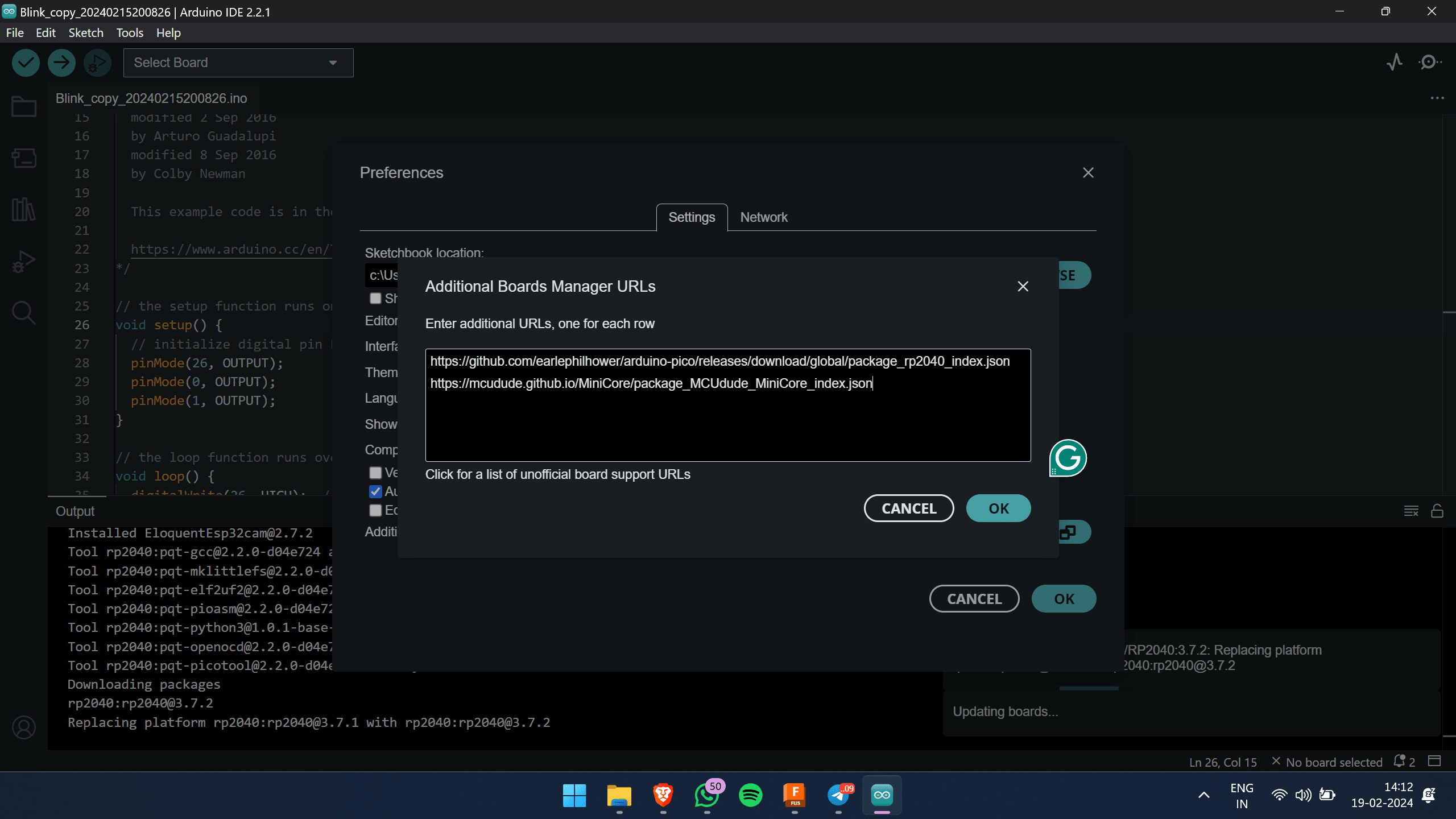
Navigate to File->Preferences. Here, we will add the URL of the additional boards
• https://github.com/earlephilhower/arduino-pico-littlefs-plugin/releases
Copy the following text and paste it into the "Additional Boards Manager URLs" field in the Preferences menu of the Arduino program
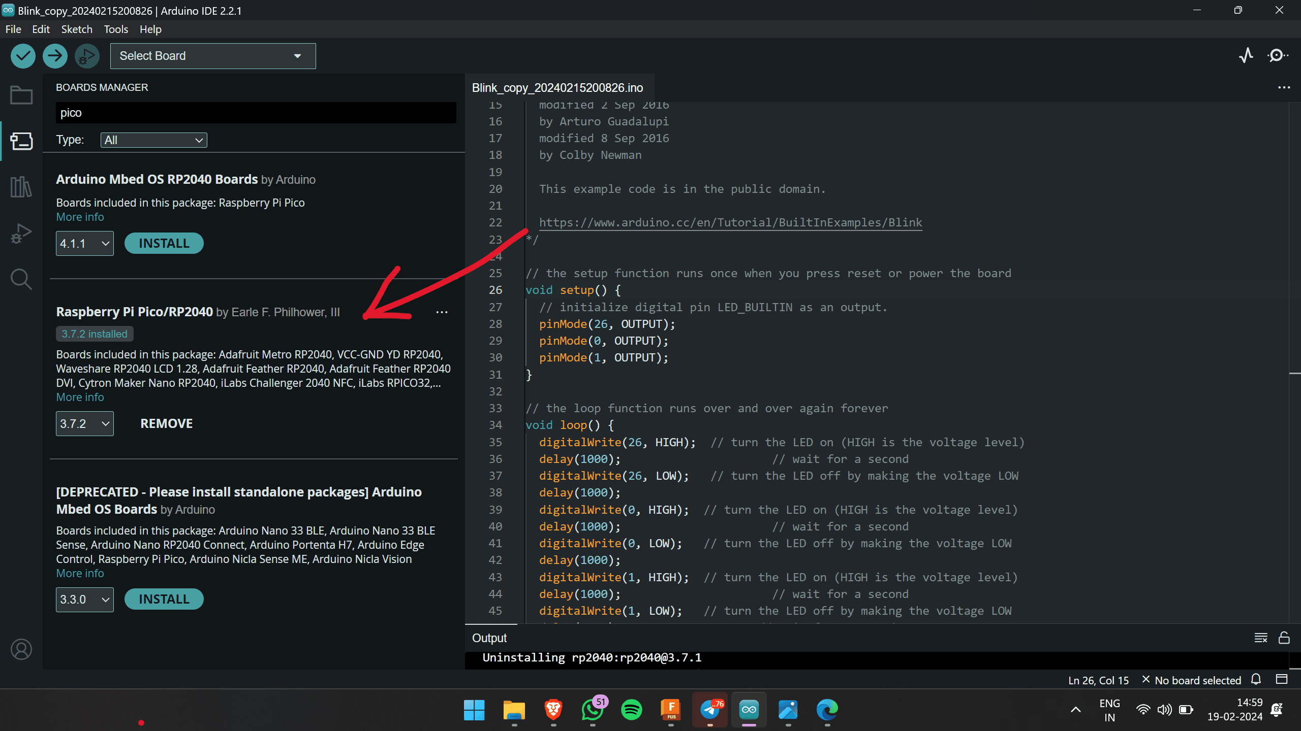
Step 2: Boards Manager
Proceed to download Pico in the boards manager. Navigate to Tools->Board->Board Manager.
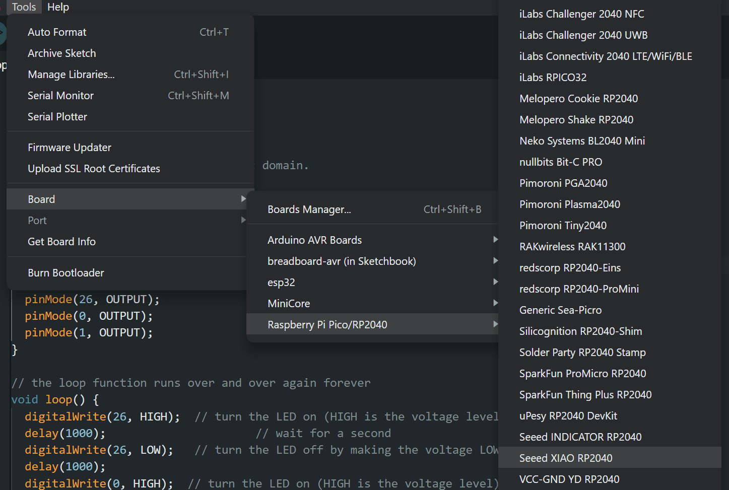
Step 3: Configure the Arduino IDE for the Seeed Studio XIAO RP2040.
Navigate to Tools->Board->Raapberry Pi Pico/RP2040- > Seeed XIAO RP2040.
The Seeed Studio XIAO RP2040 will be identified in the COM port, which in my case is COM3.
Subsequently, I commenced the coding process for the LED blink functionality. Initially, I sourced the code from examples available in the IDE platform and tailored it to meet the specific requirements for blinking the three LEDs. Below is the modified code utilized for testing the functionality of the board
void setup() {

  pinMode(26, OUTPUT);
  pinMode(0, OUTPUT);
  pinMode(1, OUTPUT);
}

// the loop function runs over and over again forever
void loop() {
  digitalWrite(26, HIGH);  // turn the LED on (HIGH is the voltage level)
  delay(1000);                      // wait for a second
  digitalWrite(26, LOW);   // turn the LED off by making the voltage LOW
  delay(1000);
  digitalWrite(0, HIGH);  // turn the LED on (HIGH is the voltage level)
  delay(1000);                      // wait for a second
  digitalWrite(0, LOW);   // turn the LED off by making the voltage LOW
  delay(1000);
  digitalWrite(1, HIGH);  // turn the LED on (HIGH is the voltage level)
  delay(1000);                      // wait for a second
  digitalWrite(1, LOW);   // turn the LED off by making the voltage LOW
  delay(1000);                    // wait for a second
}
Following the execution of the code and uploading it onto the PCB, the three LEDs commenced blinking sequentially, as intended.
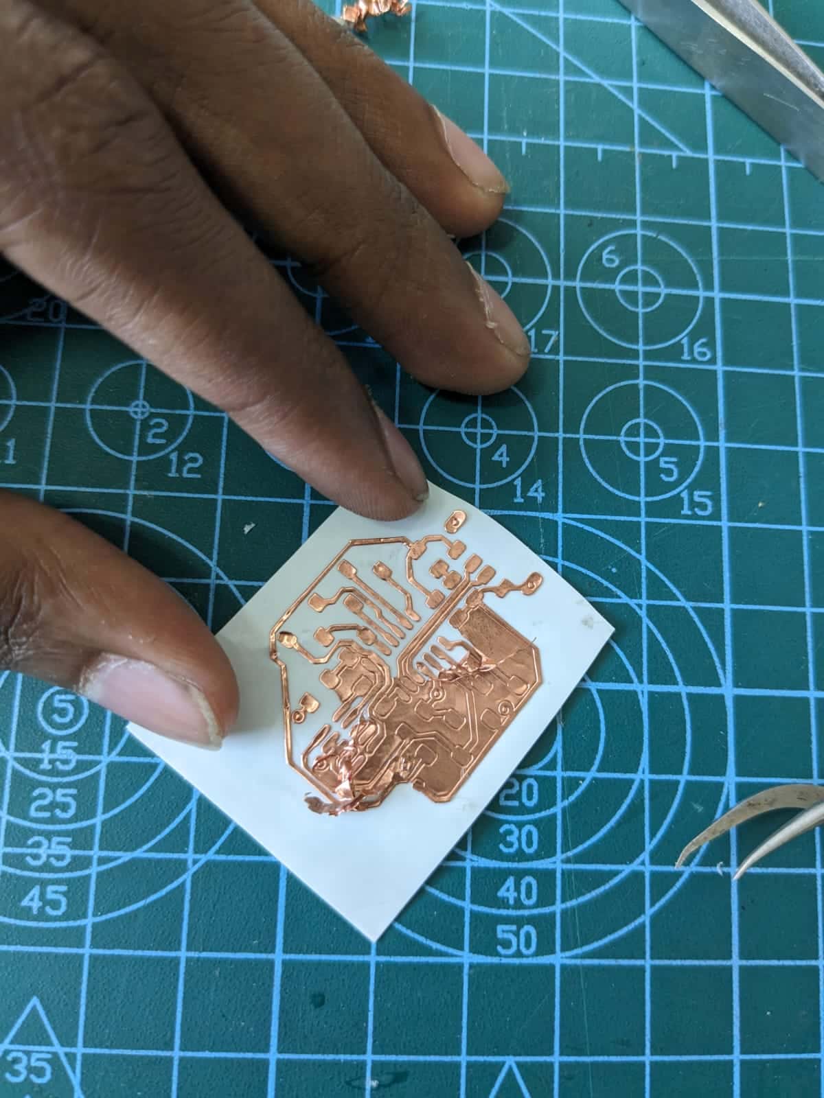
For the next fabrication method, I opted to explore vinyl cutting for trace creation.
While referring to Saheen 's fab page, I stumbled upon the SADMD11 project, originally designed by Ardian. Saheen's innovative approach involved reducing the size of the PCB. Inspired by this, I decided to adapt the project to create a flexible PCB. To do so, I utilized the files available on Saheen 's fab page. You can find more details about Saheen 's page by clicking here .
Initially, I started by cutting the design using the file obtained from Shaheen's page. Then, I proceeded to cut it with the vinyl cutter using the Fabmodes platform.
The force applied was 80gf , and the speed was set to 0.5 cm/s.
Here is the result after cutting the design in vinyl.
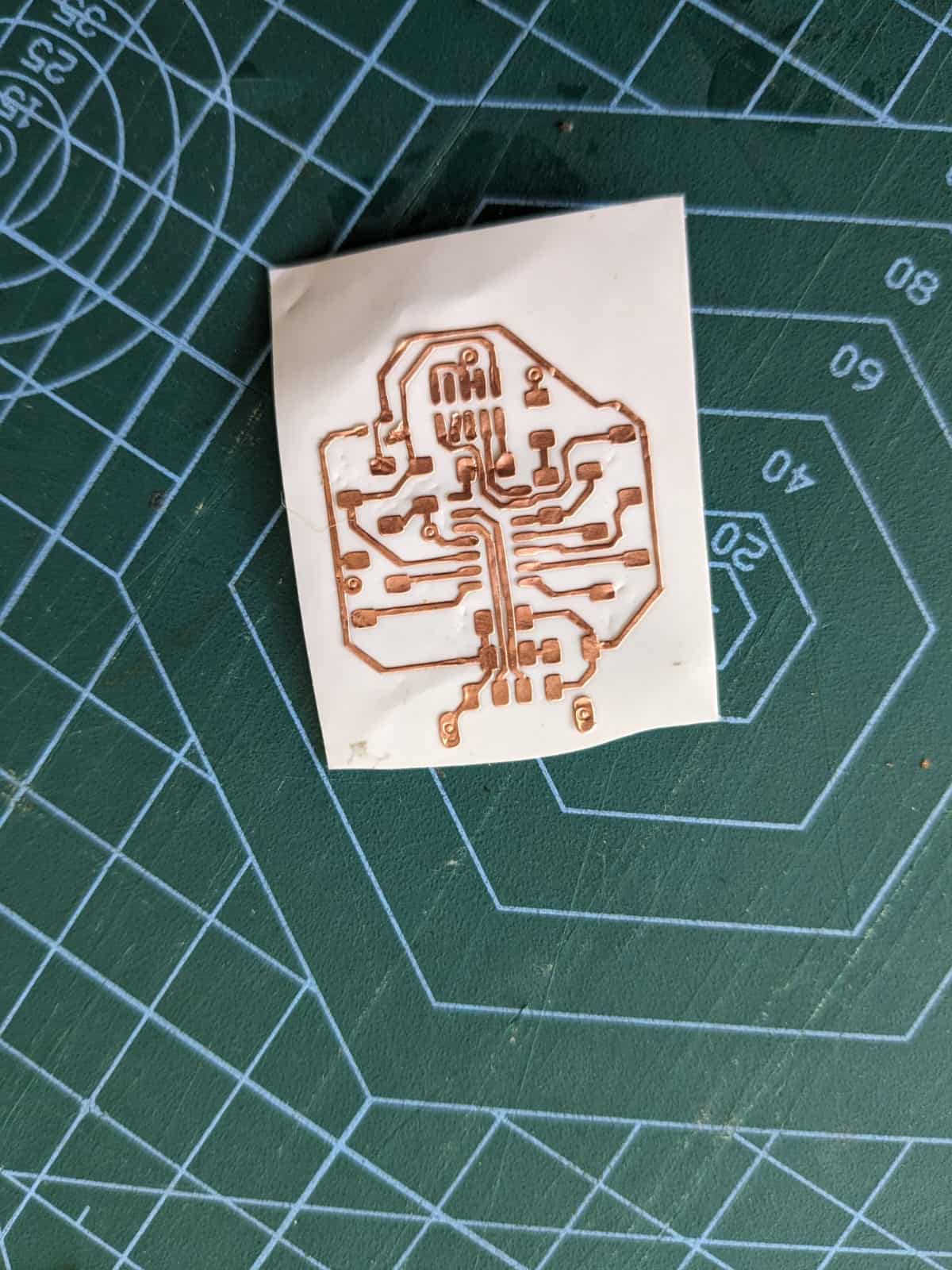
Then, I began the weeding process, which involved removing the negative parts of the vinyl design.
Here is the result after completing the weeding process.
Next, I proceeded to gather the required components from the laboratory inventory.
After gathering the required components, I began soldering them according to the instructions provided on Shaheen's Academy page.
Soldering the components onto the copper tape presented a bit of a challenge, but I managed to solder them onto it nonetheless.
And here is the result after successfully soldering the components
After successfully soldering the components, it's time to upload the code to the flexible PCB that I've created. For this step, my instructor Saheen provided valuable assistance.
Connected it to the programmer and uploaded the basic blink program from the examples. Then, edited it to specify the pin connected to the LED to initiate the blinking sequence.
Seeing the LED blinking on the flexible PCB filled me with joy and pride. It was a moment of satisfaction, knowing that the PCB was functioning as intended. I am grateful to Saheen for his invaluable assistance throughout the process.
Reflow soldering
Reflow soldering is a widely adopted process in the electronics industry for soldering surface mount components (SMCs) onto printed circuit boards (PCBs). This method involves the application of solder paste, a mixture of flux and solder powder, onto the PCB. Components are then placed on top of the solder paste, and the assembly is heated to melt the solder, creating secure electrical connections.
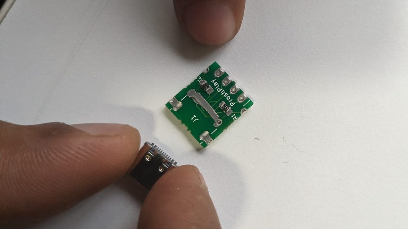
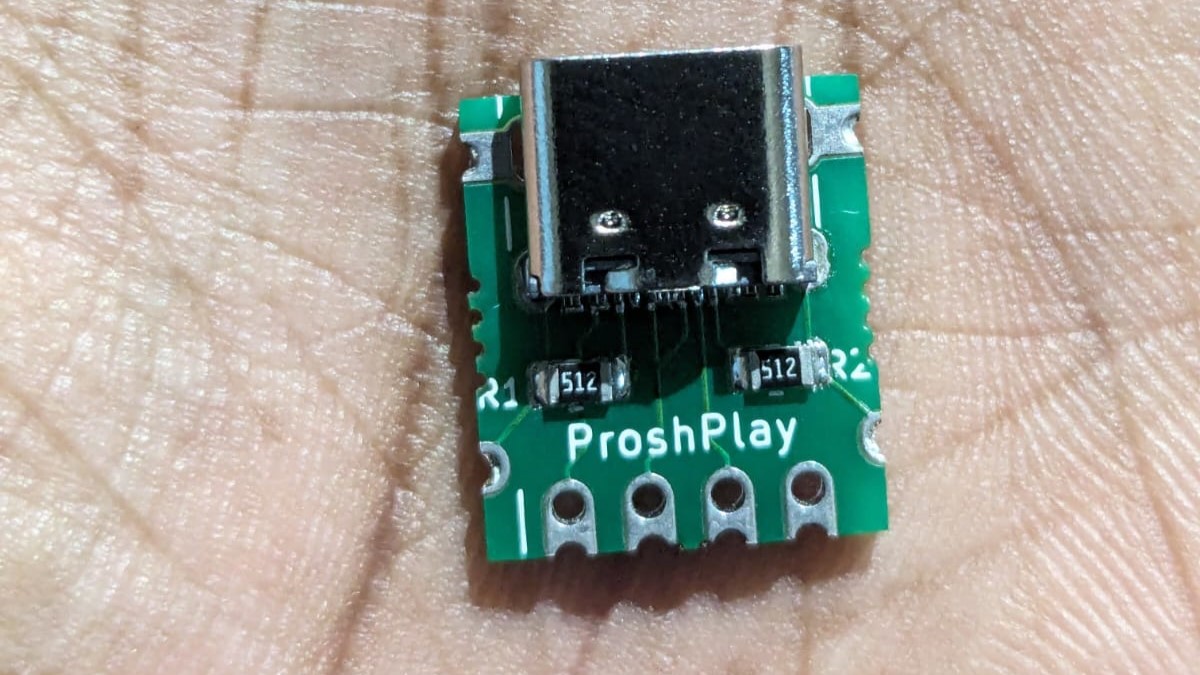
I attempted to solder a type-C jack onto the printed PCB. Due to the complexity of soldering the numerous pins on the type-C jack directly onto the PCB, I opted to use an oven to heat up the soldering paste and facilitate the soldering process.
These are the components used:
- Type-C connector
- Printed PCB provided by the lab
- Two resistors

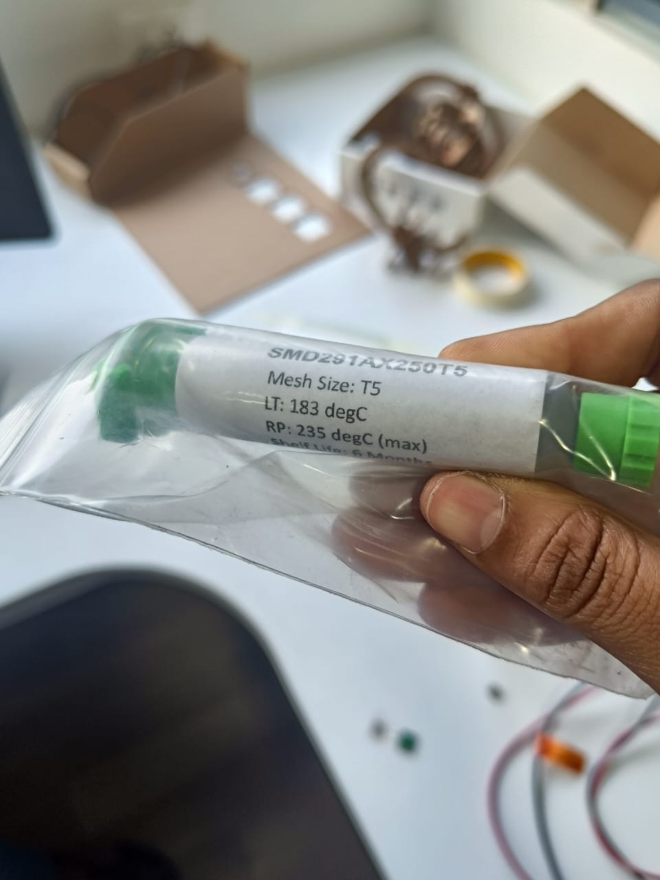
Here's the solder paste we used, along with the temperature details:
- Solder Paste: [SMD291AX250T5]
- Max temp-235 degC
Then, we created a stencil for applying the soldering paste, which was crafted by Saheen using the laser cutting machine. We utilized this stencil to apply the soldering paste, resulting in a precise and effective application.
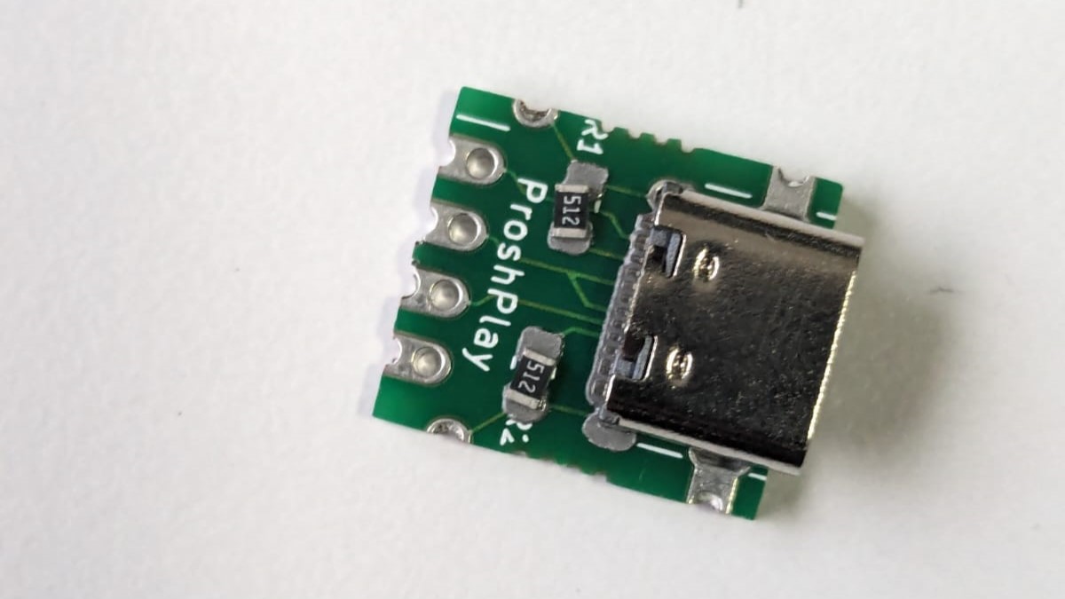
After applying the soldering paste, I carefully positioned the components onto their designated spots on the PCB. Subsequently, I placed the assembly into the oven for solder reflow.
Reflow Soldering:
Preheat Phase: During this phase, the PCB assembly is gradually heated to dry the solder paste and activate the flux. Flux, a chemical agent present in the solder paste, cleans metal surfaces to enhance the solder's bonding capability.
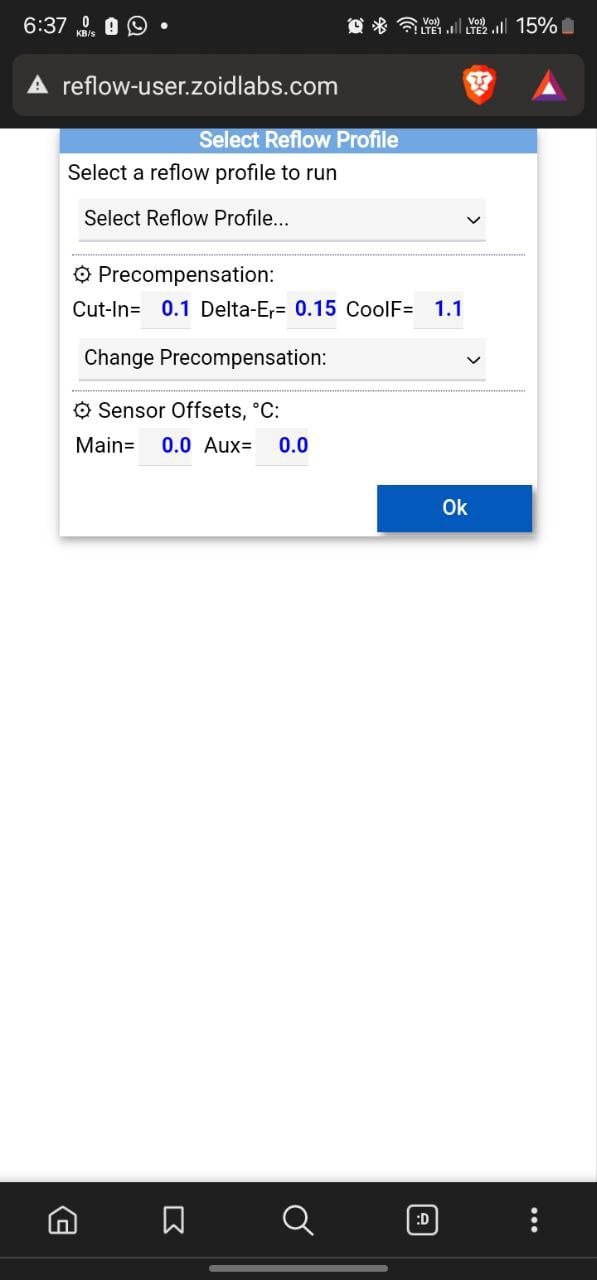
We conducted this phase using a reflow oven manufactured by a startup called "ZoidLabs."

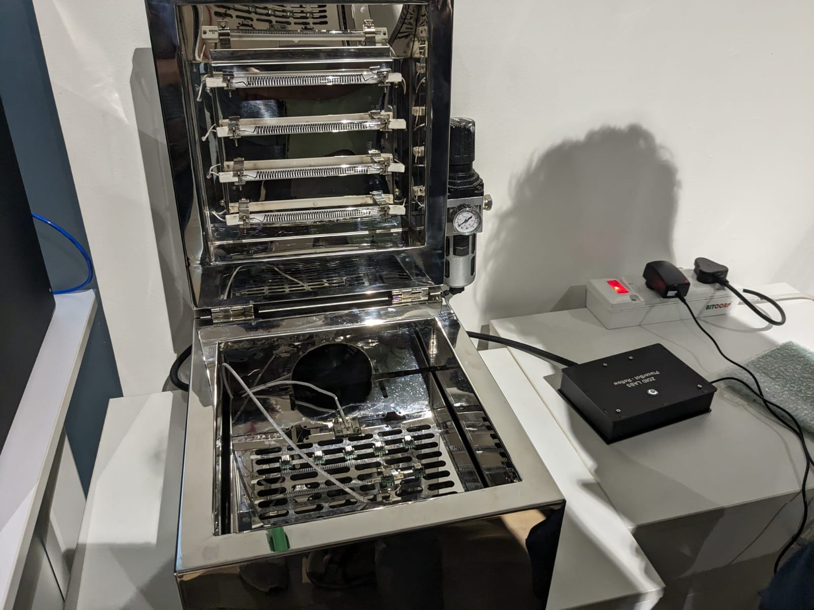
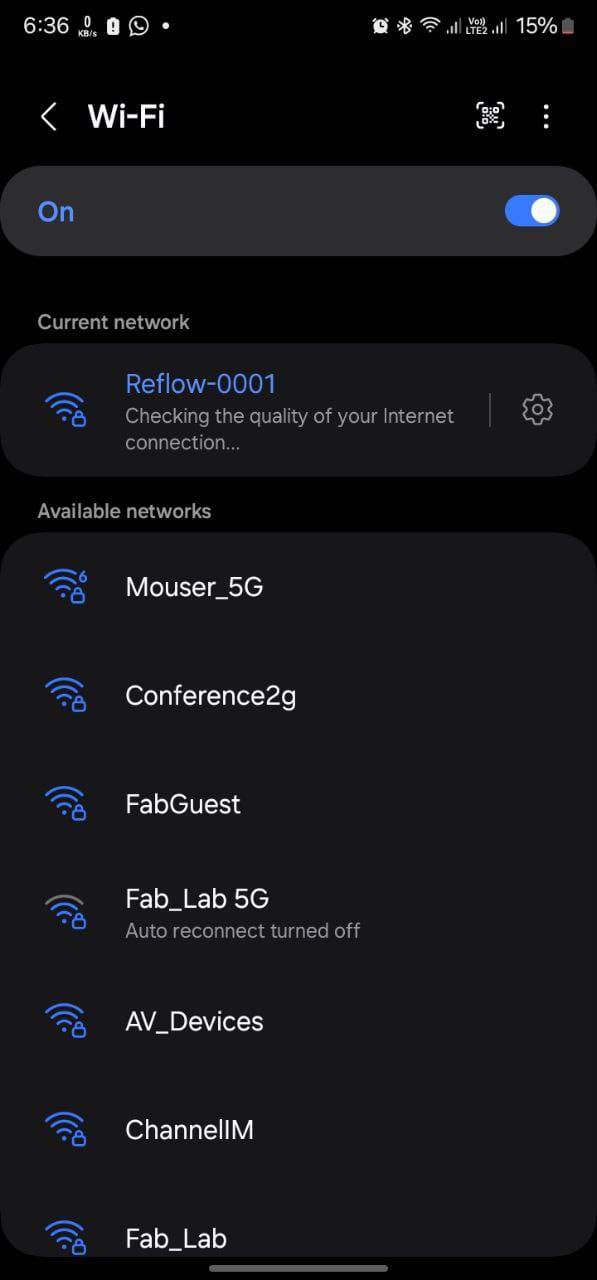
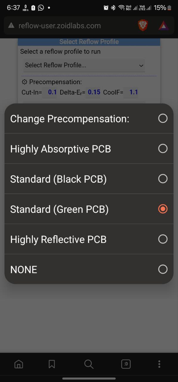
During the reflow soldering process, we utilized a reflow oven equipped with a mobile interface. This interface allowed us to connect to the device via WiFi, enabling us to monitor temperature changes throughout the different phases:
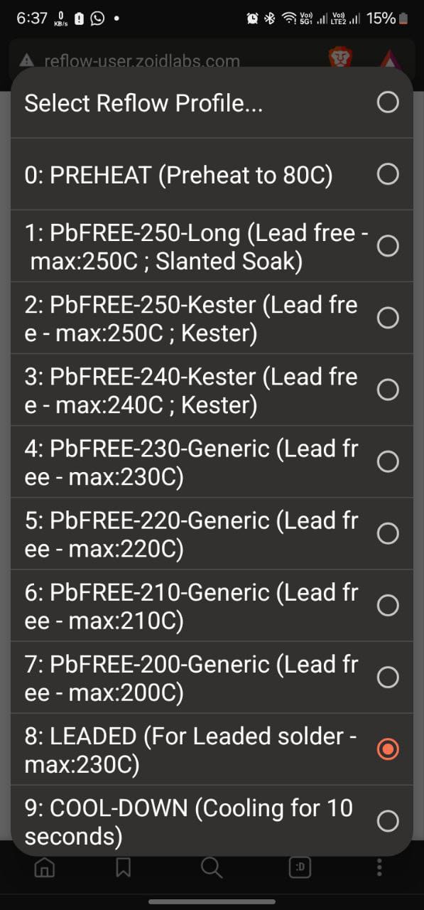
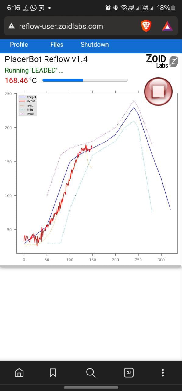
Soak Phase: In this phase, the temperature is further increased to ensure uniform heating of the entire assembly. This minimizes the risk of thermal shock to components and promotes even melting of the solder.
Reflow Phase: The temperature is raised above the melting point of the solder, typically between 183°C to 250°C (361°F to 482°F) for lead-free solder. This causes the solder paste to melt, flow, and form reliable solder joints.
Cooling Phase: Following reflow, the assembly is cooled in a controlled manner to solidify the solder, creating strong and dependable electrical and mechanical connections.
Inspection and Testing: After cooling, the solder joints are inspected for quality, ensuring they are shiny, smooth, and free from bridges or cold solder spots. The circuit is then tested to verify all connections are solid and the device functions correctly.
Safety Tips:
- Ventilation: Maintain adequate ventilation to prevent inhalation of flux fumes.
- Personal Protective Equipment (PPE): Wear safety glasses and gloves to protect against splashes and hot surfaces.
- Avoid Overheating: Monitor the temperature profile closely to avoid damaging components or the PCB.
Next, I experimented with using a hot air gun to heat the soldering paste instead of relying on the oven. This allowed me to determine which method better suited my needs and preferences.
I followed the same procedures as before, but this time, instead of using the oven, I utilized a hot air gun to heat the soldering paste.
It seems that for soldering small boards like this one, using the hot air gun is more efficient. However, if you're dealing with multiple boards, the oven might be the better choice due to its ability to handle larger quantities simultaneously.